Github Link: https://github.com/comeradealexi/MCP4131
Datasheet
One of the most important parts of programming an MCP is studying the datasheet provided with it. For the MCP4131, you can download it here: https://www.microchip.com/en-us/product/MCP4131
It will provide everything you need to know about the chip. One of the most basic pieces of information we’ll need to start with is what each pin on the chip does:
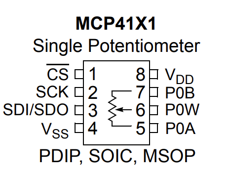
CS = Chip Select
SCK = Serial Clock
SDI/SDO = Serial Data In / Serial Data Out
VSS = Ground
VDD = Positive Power Supply Input
P0B = Potentiometer Terminal B
P0W = Potentiometer Wiper (W) Terminal
P0A = Potentiometer Terminal A
Pin Input/Output Protocol
Below is a diagram from the datasheet showing you the protocol for each pin in order to program the MCP4131.
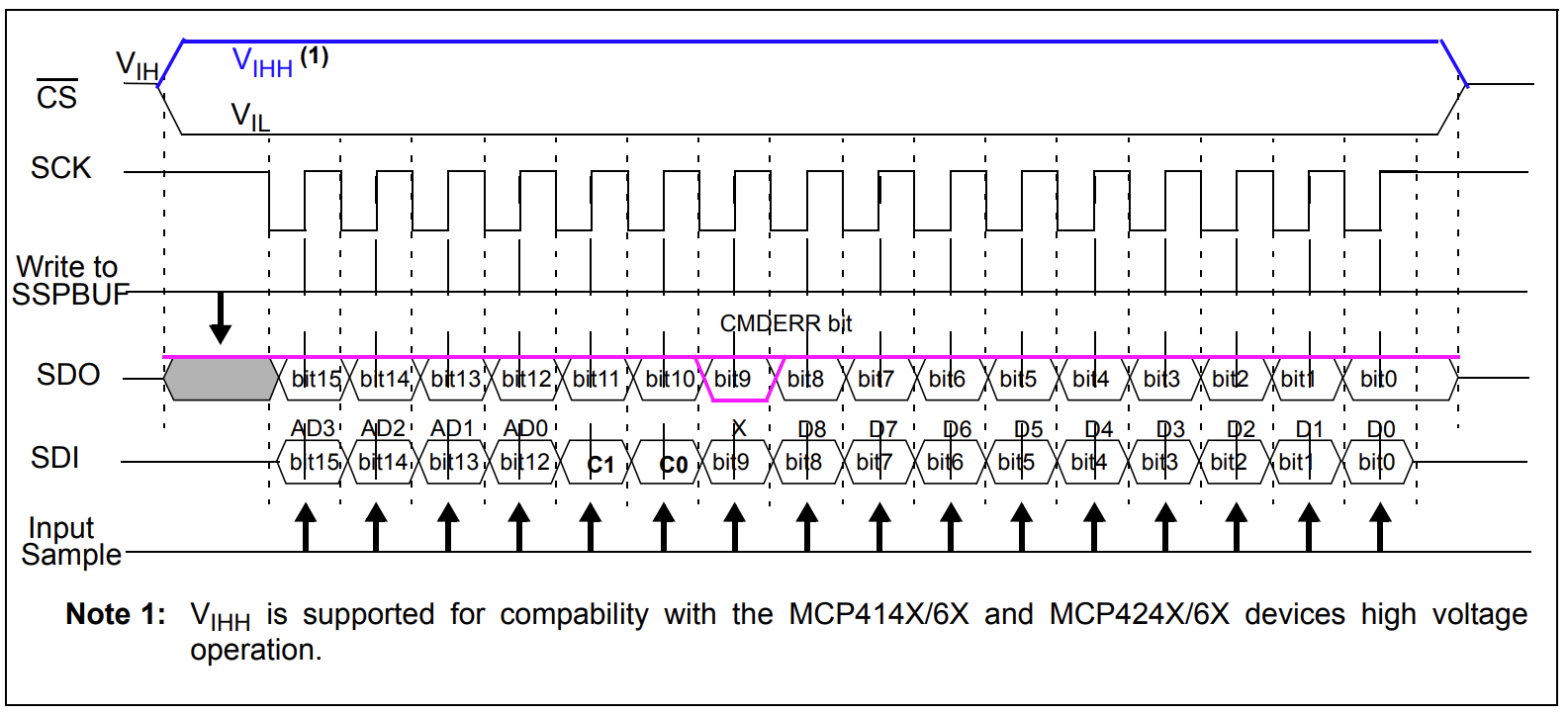
Initial state of all pins:
- CS = HIGH
- SCK = HIGH
- SDI/SDO = LOW
(HIGH = 3.3 Volts, GPIO ON)
(LOW = 0 Volts, GPIO OFF)
SDI Bit Layout
The MCP4131 expects 16 bits of data to be passed each time we program it. The layout of these 16 bits are as follows:

In our case the MCP4131 is a 7-bit device which means our Data Byte supports just 7 bits… Which means we can program it with values between 0 and 127. Where 0 would be full resistance and 127 being no resistance.
In this case, our memory bits should all be 0, our commands bits should be 0 0 as we’re writing data and the first 3 data bits also 0 because it’s a 7 bit potentiometer. So the first 9 bits we write should all be zeros.
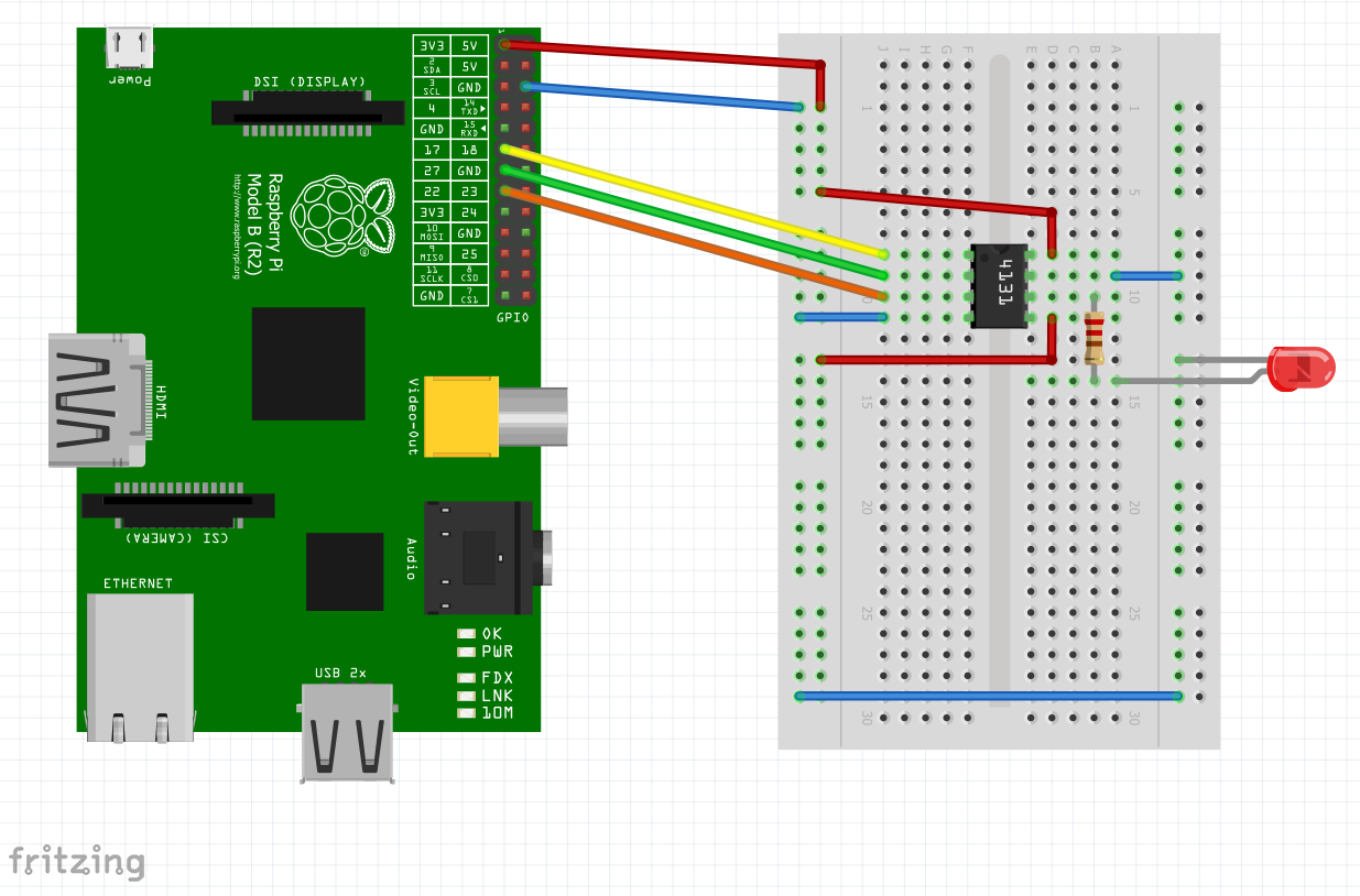
PCB Setup
GPIO 17 = CS
GPIO 27 = CLK
GPIO 22 = SDI/SDO
The LED is connected to the Potentiometer Wiper.
Source Code
https://github.com/comeradealexi/MCP4131 – The code here will cycle from max to min then back to max again.
The initial setup code here initialises WiringPi and sets the pins as outputs and also puts all of our output pins into their default states.
	MCP4131(int inGPIO_CS, int inGPIO_SCK, int inGPIO_SDI) : GPIO_CS(inGPIO_CS), GPIO_SCK(inGPIO_SCK), GPIO_SDI(inGPIO_SDI)
	{
		wiringPiSetupSys();

		pinMode(GPIO_CS, OUTPUT);
		pinMode(GPIO_SCK, OUTPUT);
		pinMode(GPIO_SDI, OUTPUT);


		digitalWrite(GPIO_CS, LOW);
		digitalWrite(GPIO_SCK, LOW);
		digitalWrite(GPIO_SDI, LOW);

		digitalWrite(GPIO_CS, HIGH);
		digitalWrite(GPIO_SCK, LOW);
		digitalWrite(GPIO_SDI, LOW);
	}
Once the setup is complete, the chip is programmed via the WriteData function.
	//7 bit values 0-127
	void WriteData(unsigned char Value)
	{
		const int DelayTime = 10;

		if (Value > 127) Value = 127; //Clamp to 7 bit max value

		digitalWrite(GPIO_CS, LOW);
		delayMicroseconds(DelayTime);

		for (int i = 0; i < 16; i++)
		{
			bool bHigh = false; //First 9 bits are all 0

			//Write out the last 7 data bits (MSB fist)
			if (i > 8)
			{
				unsigned char idx = (i - 9); //6 to 0
				unsigned char bit = 1 << (6 - idx);
				bHigh = Value & bit;
			}

			digitalWrite(GPIO_SDI, bHigh ? HIGH : LOW);
			digitalWrite(GPIO_SCK, HIGH);
			delayMicroseconds(DelayTime);
			digitalWrite(GPIO_SCK, LOW);
			delayMicroseconds(DelayTime);
		}

		digitalWrite(GPIO_CS, HIGH);
	}
The code matches the protocol image we saw earlier. We start by setting the Chip Select (CS) to low, this tells the chip we are going to start writing to it.
We then start writing our 16 bits of data. Setting out desired bit and then setting the SCK to HIGH and back to low again to complete the writing of a single bit. This is done 16 times in total.
After the last bit is written, we set the CS back to HIGH and that completes the data writing!
Leave a Reply